NPS System(New Plasma Source System)은 고밀도 Plasma Beam을 기반으로
고효율의 Perovskite Solar Cell 생산을 위한 투명 전도성 산화물(TCO) 증착 설비입니다.
New Plasma
Source System
경쟁력
-
Point 01
전문 엔지니어들의 다년 간의 R&D로 터득한
Know-how를 통해 최적의 H/W 설계 및 공정 Consulting 제공
(R&D System 및 Measuring instrument 보유)
-
Point 02
우수한 성능 및 생산성을 기반으로 Solar Cell 시장 내
다양한 Big Customer를 대상으로 Sales Reference 보유
New Plasma
Source
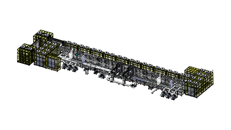
2,400x1,200mm 대면적 Perovskite Solar Cell 용 저온 증착 설비

Technology
Advantages of
NPS Process
NPS
New Plasma Source
-
Smooth Surface
Super Smooth Surface Performance
(Better Performance for Down Stream Process) -
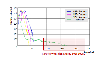
Low Temperature & Plasma Damage
Prevent degradation of
sub-layer by heat and plasma -
High Productivity
Continuous production through source
material supply without vacuum breakHigh yield by superior system stability & reliability
Easy Preventive Maintenance
-
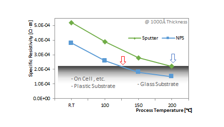
Excellent Film Quality
High quality of electrical &
optical properties than sputtering process